
Type 2N4150
Geometry
9201
Polarity NPN
Qual Level: JAN - JANTXV
Data Sheet No. 2N4150
Generic Part Number:
2N4150
REF: MIL-PRF-19500/394
Features:
∑
Power switching transistor for high
speed switching applicatons.
∑
Housed in a
TO-5
case.
∑
Also available in chip form using
the
9201
chip geometry.
∑
The Min and Max limits shown are
per
MIL-PRF-19500/394
which
Semicoa meets in all cases.
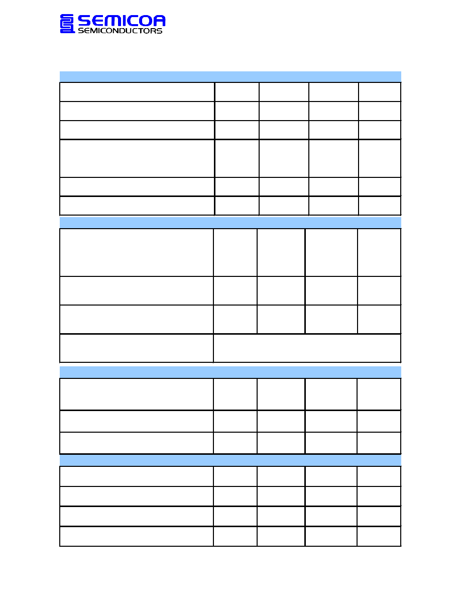
Rating
Symbol
Rating
Unit
Collector-Emitter Voltage
V
CEO
70
V
Collector-Base Voltage
V
CBO
100
V
Emitter-Base Voltage
V
EBO
10
V
Collector Current, Continuous
I
C
10
A
Power Dissipation at 25
o
C ambient
1.0
mW
Derate above 25
o
C
5.7
mW/
o
C
Power Dissipation at 25
o
C ambient
5.0
W
Derate above 25
o
C
50
mW/
o
C
R
JC
0.020
o
C/mW
R
JA
0.175
o
C/mW
Operating Junction Temperature
T
J
-65 to +200
o
C
Storage Temperature
T
STG
-65 to +200
o
C
Thermal Impedance
Maximum Ratings
T
C
= 25
o
C unless otherwise specified
P
T
P
T
TO-5
Data Sheet No. 2N4150
OFF Characteristics
Symbol
Min
Max
Unit
Collector-Base Breakdown Voltage
I
C
= 10 µA
Collector-Emitter Breakdown Voltage
I
C
= 0.1 A, pulsed
Emitter-Base Breakdown Voltage
I
E
= 10 µA
Collector-Emitter Cutoff Current
V
CE
= 60 V
I
CEO1
---
10
µA
V
BE
= 0.5 V, V
CE
= 100 V
I
CEX
---
10
µA
V
BE
= -0.5 V, V
CE
= 80 V, T
C
= +150
o
C
I
CEX2
100
µA
Emitter-Base Cutoff Current
V
EB
= 5V
Collector-Base Cutoff Current
V
CB
= 80 V
I
CBO
---
0.1
µA
µA
V
Electrical Characteristics
T
C
= 25
o
C unless otherwise specified
V
V
V
(BR)CBO
100
---
I
EBO
---
0.1
V
(BR)CEO
70
---
V
(BR)EBO
7.0
---
ON Characteristics
Symbol
Min
Max
Unit
Forward current Transfer Ratio
I
C
= 1 A, V
CE
= 5 V, pulsed
h
FE1
50
200
---
I
C
= 5 A, V
CE
= 5.0 V, pulsed
h
FE2
40
120
---
I
C
= 10 A, V
CE
= 5 V
h
FE3
10
---
---
I
C
= 5 A, V
CE
= 5.0 V, T
C
= -55
o
C
h
FE4
20
---
---
Collector-Emitter Saturation Voltage
I
C
= 5 A, I
B
= 0.5 A pulsed
V
CE(sat)1
---
0.6
V dc
I
C
= 10 A, I
B
= 1 A, pulsed
V
CE(sat)2
---
2.5
V dc
Base-Emitter Saturation Voltage
I
C
= 5 A, I
B
= 0.5 A, pulsed
V
BE(sat)1
---
1.5
V dc
I
C
= 10 A, I
B
= 1 A, pulsed
V
BE(sat)2
---
2.5
V dc
Safe Operating Area, Continuous DC
V
CE
= 40 V, I
C
= 0.22 A
V
CE
= 70 V, I
C
= 90 mA
T
C
= 25
o
C, t = 1.0 s
Small Signal Characteristics
Symbol
Min
Max
Unit
Magnitude of Common Emitter Small Signal
Short Circuit Forward Current Transfer Ratio
V
CE
= 10 V, I
C
= 0.2 A, f = 10 MHz
Open Circuit Output Capacitance
V
CB
= 10 V, I
E
= 0, 100 kHz < f < 1 MHz
Small Signal, Short Circuit, Forward Current
V
CE
= 10 V, I
C
= 50 mA, f = 1 kHz
---
|h
fe
|
1.5
7.5
pF
C
OBO
---
350
h
fe
40
160
---
Switching Characteristics
Symbol
Min
Max
Unit
Delay Time
Per Figure 4, MIL-PRF-19500/394C
Rise Time
Per Figure 4, MIL-PRF-19500/394C
Storage Time
Per Figure 4, MIL-PRF-19500/394C
Fall Time
Per Figure 4, MIL-PRF-19500/394C
ns
t
d
---
50
t
r
---
500
ns
t
s
---
1.5
ns
t
f
---
50
ns